Scanning Electron Microscope
Scanning Electron Microscope
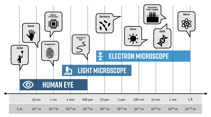
A scanning electron microscope (SEM) is an electron microscope that produces images of a sample by scanning the surface with a focused beam of electrons. The electrons interact with atoms in the sample, producing various signals that contain information about the surface topography and composition of the sample. The electron beam is scanned in a raster scan pattern, and the beam's position is combined with the intensity of the detected signal to produce an image. In the most common SEM mode, secondary electrons emitted by atoms excited by the electron beam are detected using a secondary electron detector (Everhart–Thornley detector). The number of secondary electrons that can be detected, and thus the signal intensity, depends, among other things, on specimen topography. Some SEMs can achieve resolutions better than 1 nanometer.
The first Scanning Electron
Microscope was initially made by Mafred von Ardenne
in 1937 with an aim to surpass the transmission electron Microscope. He used
high-resolution power to scan a small raster using a beam of electrons that
were focused on the raster. He also aimed at reducing the problems of chromatic
aberrations images produced by the Transmission electron Microscopes. More
studies followed by scientists and research institutions such as Cambridge
Scientific Instrument Company who eventually developed a fully constructed
Scanning electron Microscope, in 1965 and named it a Stereoscan. The
price of the Scanning Electron Microscope (SEM) is approximately $1 million.
Specimens are observed in high vacuum in a conventional SEM, or in low vacuum or wet conditions in a variable pressure or environmental SEM, and at a wide range of cryogenic or elevated temperatures with specialized instruments.

|
Accelerating Voltage |
Type of Electron Microscope |
Electron Wavelength, λ |
|
5 kV |
SEM |
0.0172 nm |
|
10 kV |
0.0122 nm |
|
|
20 kV |
0.0086 nm |
|
|
200 kV |
TEM/STEM |
0.0027 nm |
Scanning
Electron Microscope (SEM) Definition
Scanning Electron Microscope (SEM) is
a type of electron microscope that scans surfaces of microorganisms that uses a
beam of electrons moving at low energy to focus and scan specimens. The
development of electron microscopes was due to the inefficiency of the
wavelength of light microscopes. electron microscopes have very short
wavelengths in comparison to the light microscope which enables better
resolution power.
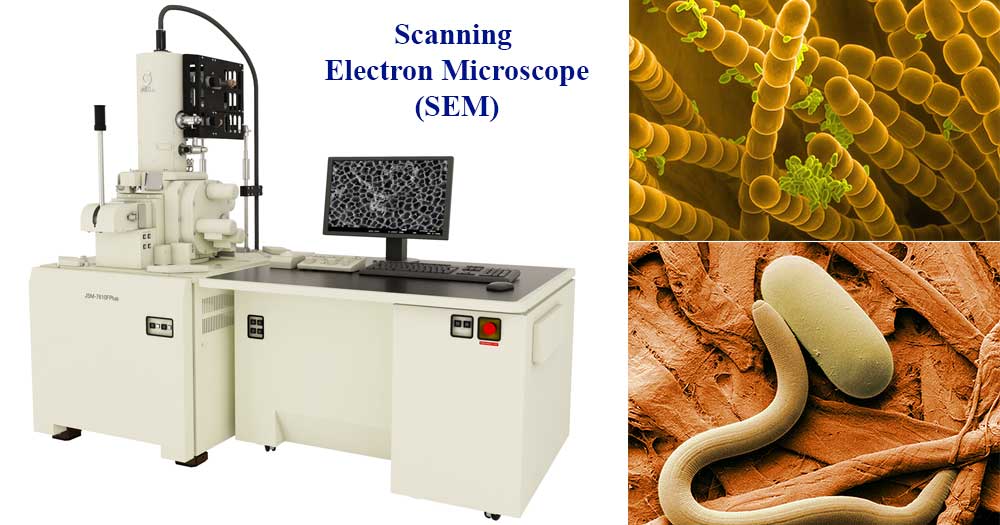
Image Source: JEOL USA, Inc. and Wikipedia.
History
An account of the early history of scanning electron microscopy has been presented by McMullan. Although Max Knoll produced a photo with a 50 mm object field width showing channeling contrast by the use of an electron beam scanner, it was Manfred von Ardenne who in 1937 invented a microscope with high resolution by scanning a very small raster with a demagnified and finely focused electron beam. In the same year, Cecil E. Hall also completed the construction of the first emission microscope in North America, just 2 years after being tasked by his supervisor, E. F. Burton at the University of Toronto. Ardenne applied scanning of the electron beam in an attempt to surpass the resolution of the transmission electron microscope (TEM), as well as to mitigate substantial problems with chromatic aberration inherent to real imaging in the TEM. He further discussed the various detection modes, possibilities and theory of SEM, together with the construction of the first high-resolution SEM. Further work was reported by Zworykin's group, followed by the Cambridge groups in the 1950s and early 1960s headed by Charles Oatley, all of which finally led to the marketing of the first commercial instrument by Cambridge Scientific Instrument Company as the "Stereoscan" in 1965, which was delivered to DuPont.
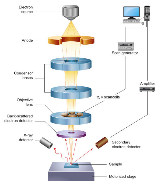
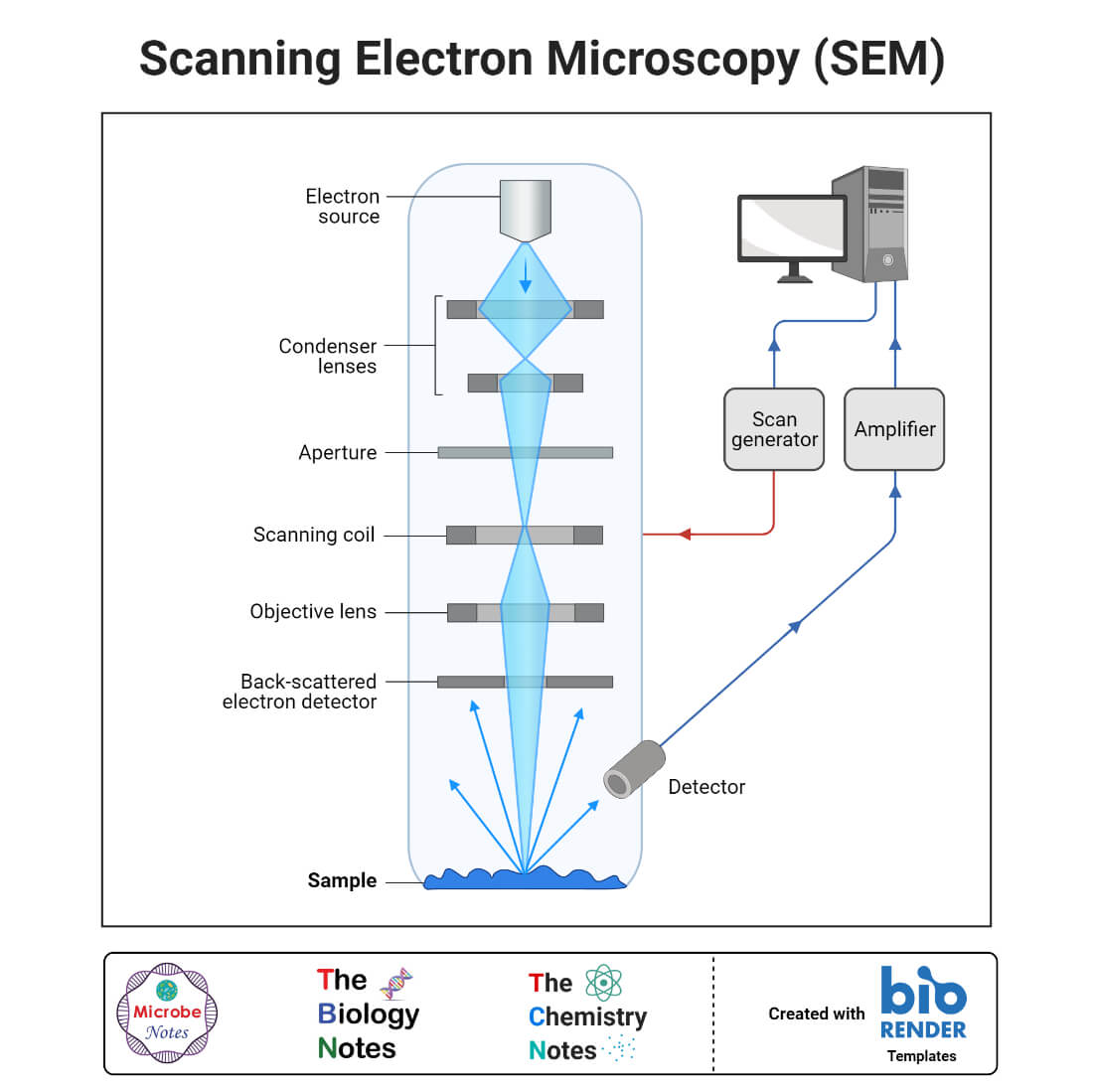
Components in a SEM
The main SEM components include:
- Electron source (gun)
- Condenser lenses
- Objective lens
- X-Y scan coils & scan generator
- Detectors
- Sample stage
- Computer and display to view the images
- External vacuum pump(s)
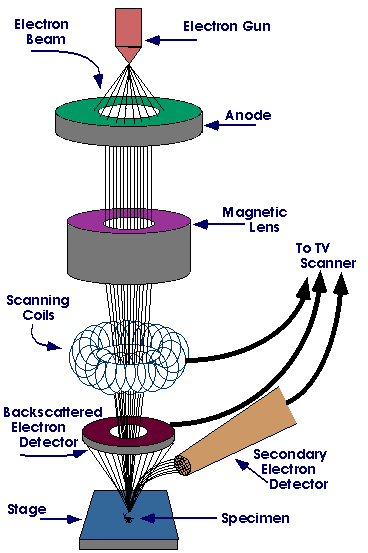
Principle
of Scanning Electron Microscope (SEM)
Unlike the Transmission Electron Microscope
which uses transmitted electrons, the scanning electron Microscope uses emitted
electrons. The Scanning electron microscope works on the principle of
applying kinetic energy to produce signals on the interaction of the electrons.
These electrons are secondary electrons, backscattered electrons, and
diffracted backscattered electrons which are used to view crystallized elements
and photons. Secondary and backscattered electrons are used to produce an image.
The secondary electrons are emitted from the specimen play the primary role of
detecting the morphology and topography of the specimen while the backscattered
electrons show contrast in the composition of the elements of the specimen.
How
does the Scanning Electron Microscope (SEM) work?
- The source of the electrons and the electromagnetic lenses are from tungsten filament lamps that are placed at the top of the column and it is similar to those of the transmission electron Microscope.
- The electrons are emitted after thermal energy is applied to the electron source and allowed to move in a fast motion to the anode, which has a positive charge.
- The beam of electrons activates the emission of primary scattered (Primary) electrons at high energy levels and secondary electrons at low-energy levels from the specimen surface. The beam of electrons interacts with the specimen to produce signals that give information about the surface topography and composition of the specimen.
- The specimen does not need special treatment for visualization under the SEM, even air-dried samples can be examined directly. However, microbial specimens need fixation, dehydration, and drying in order to maintain the structural features of the cells and to prevent collapsing of the cells when exposed to the high vacuum of the microscope.
- The samples are mounted and coated with thin layer of heavy metal elements to allow spatial scattering of electric charges on the surface of the specimen allowing better image production, with high clarity.
- Scanning by this microscope is attained by tapering a beam of electrons back and forth over a thin section of the microscope. When the electrons reach the specimen, the surface releases a tiny staw of electrons known as secondary electrons which are then trapped by a special detector apparatus.
- When the secondary electrons reach and enter the detector, they strike a scintillator (a luminescence material that fluoresces when struck by a charged particle or high-energy photon). This emits flashes of light which get converted into an electric current by a photomultiplier, sending a signal to the cathode ray tube. This produces an image that looks like a television picture that can be viewed and photographed.
- The quantity of secondary electrons that enter the detector is highly defined by the nature of the specimen i.e raised surfaces to receive high quantities of electrons, entering the detector while depressed surfaces have fewer electrons reaching the surface and hence fewer electrons enter the detector.
- Therefore raised surfaces will appear brighter on the screen while depressed surfaces appear darker.
Parts
of a Scanning Electron Microscope (SEM)
The major components of the Scanning Electron
Microscope include;
- Electron Source – This is where electrons are produced under thermal heat at a voltage of 1-40kV. the electrons condense into a beam that is used for the creation of an image and analysis. Three types of electron sources can be used i. e Tungsten filament, Lanthanum hexaboride, and Field emission gun (FEG)
- Lenses – it has several condenser lenses that focus the beam of electrons from the source through the column forming a narrow beam of electrons that form a spot called a spot size.
- Scanning Coil – they are used to deflect the beam over the specimen surface.
- Detector – It’s made up of several detectors that can differentiate the secondary electrons, backscattered electrons, and diffracted backscattered electrons. The functioning of the detectors highly depends on the voltage speed, and the density of the specimen.
- The display device (data output device)
- Power supply
- Vacuum system
Like the transmission electron Microscope, the
Scanning electron microscope should be free from vibrations and any
electromagnetic elements.
Scanning
Electron Microscope (SEM) Images
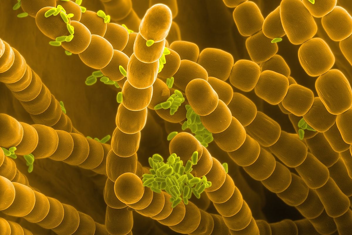
Figure: SEM image of Tradescantia pollen and
stamens. Source: Wikipedia

Figure: Low-temperature scanning electron micrograph of soybean cyst nematode and its egg. Magnified 1,000 times. Source: Wikipedia
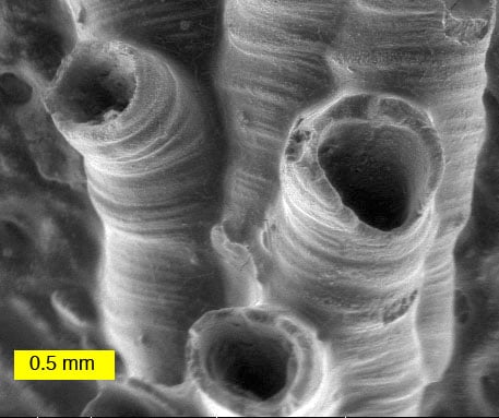
Figure: Scanning electron microscope image of a hederelloid from the Devonian of Michigan (largest tube diameter is 0.75 mm). Source: Wikipedia.
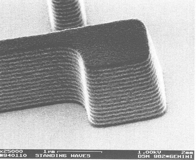
Figure: Photoresist SEM micrograph (1995) SEM= DSM 982 Gemini from Zeiss. Source: Wikipedia.
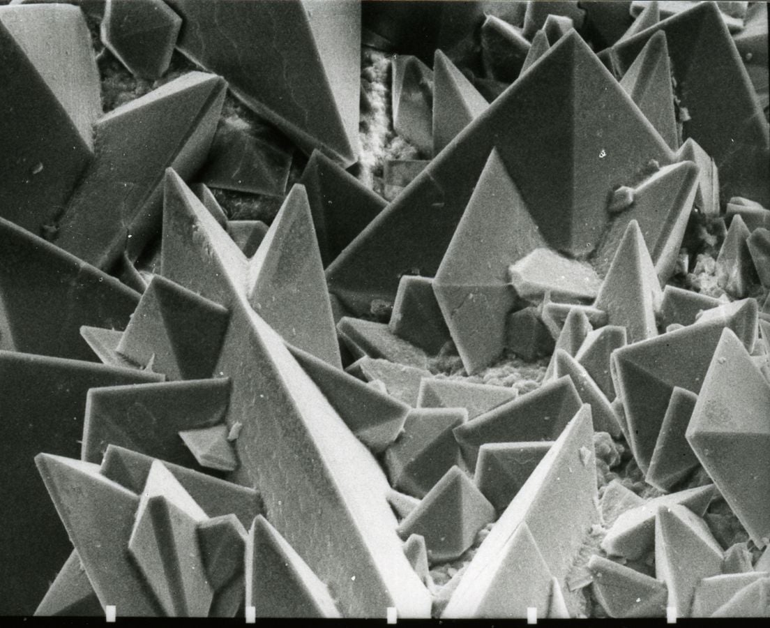
Figure: Scanning Electron Micrograph of the surface of a kidney stone showing tetragonal crystals of Weddellite (calcium oxalate dihydrate) emerging from the amorphous central part of the stone. Source: Wikipedia.
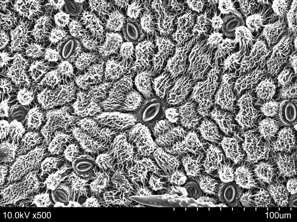
Figure: SEM image of stomata on the lower
surface of a leaf. Source: Wikipedia.
Applications
of the Scanning Electron Microscope (SEM)
It is used in a variety of fields including
Industrial uses, nanoscience studies, Biomedical studies, Microbiology
- Used for spot chemical analysis in energy-dispersive X-ray Spectroscopy.
- Used in the analysis of cosmetic components which are very tiny in size.
- Used to study the filament structures of microorganisms.
- Used to study the topography of elements used in industries.
Advantages
of the Scanning Electron Microscope (SEM)
- They are easy to operate and have user-friendly interfaces.
- They are used in a variety of industrial applications to analyze surfaces of solid objects.
- Some modern SEMs are able to generate digital data that can be portable.
- It is easy to acquire data from the SEM, within a short period of about 5 minutes.
Limitations
- They are very expensive to purchase
- They are bulky to carry
- They must be used in rooms that are free of vibrations and free of electromagnetic elements
- They must be maintained with a consistent voltage
- They should be maintained with access to cooling systems
The
combination of the working principles of the Scanning Electron Microscope (SEM)
and the Transmission Electron Microscope (TEM) formed the Scanning-Transmission
Electron Microscope (STEM). The Scanning- Transmission Electron
Microscope (STEM), uses a convergent beam of electrons to focus on a probe on
the specimen, and the probe is then scanned on its surface collecting signals
which are then collected as point-to-point to form an image.
References
- Microbiology by Lansing M. Prescott
- https://serc.carleton.edu/research_education/geochemsheets/techniques/SEM.html
- https://www.britannica.com/technology/scanning-electron-microscope
- https://blog.phenom-world.com/what-is-sem
- https://www.atascientific.com.au/sem-imaging-applications-practical-uses-scanning-electron-microscopes/
Sources
- https://serc.carleton.edu/research_education/geochemsheets/techniques/SEM.html
- https://www.youtube.com/watch?v=qExUDTqi8Xc
- https://www.nrel.gov/materials-science/scanning-transmission.html
- https://www.mse.iastate.edu/research/sem/microscopy/how-does-the-sem-work/high-school/how-the-sem-works/backscattered-electrons/
- https://www.jeol.co.jp/en/applications/pdf/sm/sem_atoz_all.pdf
- https://www.britannica.com/technology/scanning-electron-microscope
- https://www.advance-africa.com/KCSE-Biology-Questions-and-Answers.html
- https://warwick.ac.uk/fac/sci/physics/current/postgraduate/regs/mpagswarwick/ex5/techniques/structural/tem/
- https://sciencing.com/advantages-transmission-electron-microscope-6309088.html
- https://en.wikipedia.org/wiki/Scanning_electron_microscopy
- https://en.wikipedia.org/wiki/Scanning_electron_microscope
- https://courses.lumenlearning.com/microbiology/chapter/staining-microscopic-specimens/
- https://www.britannica.com/technology/microscope
- https://wikimili.com/en/Neutron_detection
- https://quizlet.com/70441933/chapters-5-6-exposures-2-flash-cards/
- https://quizlet.com/122654377/chapter-9-the-x-ray-tube-flash-cards/
- https://quizlet.com/101643159/chapter-2-x-ray-beam-flash-cards/
- https://archiveshub.jisc.ac.uk/data/gb12-ms.csic
- http://wps.prenhall.com/chet_saferstein_forensicscience_1/59/15205/3892732.cw/-/3892734/index.html


Comments
Post a Comment