Electron Beam Lithography
Lithography
Lithography comes from the Greek words lithos means stone and grapho means write. Low dimensional structures are defined with writing patterns at micro/nano-meter scale designed by printing text or graphics on the surface of materials. Lithography is currently one of the most feasible techniques used for patterning micro/nanoscale features of desired designs with definite shapes, sizes and material compositions, selectively on the material of choice for device fabrication. Several lithographic methods are developed with different resolutions, reproducibility, speed, simplicity for processing, acquisition costs, etc., by using different sources of energy. The process of utilizing a light source for patterning is termed as photolithography and the utilization of energetic beams as a source is nomenclatured according to the type of energy source.
During semiconductor processing, the fabrication of micro/nano-structures rearranges the additives by deposition, subtractives by etching, and surface dopants by annealing. Etching out unwanted materials and depositing desired materials for the fabrication of a complete nanostructure or device structure is the key concept of microfabrication processing. Lithography is used for defining the wanted and unwanted regions by using a polymer chemical called a resist layer over top of the surface to be patterned. The etching of unwanted material or metallization of new materials is pursued with the patterned resist on the surface, followed by resist cleaning to fabricate the desired structure. Simple solvents includes acetone, methyl ethyl ketone (CH3COC2H5), methyl isobutyl ketone (CH3COC4H9) for chemicals used for resists stripping/lift-off process. Additional O2 plasma cleaning is effective for removing residual resist or any organic contaminations during a lithography process.
- Types of Lithography
Table: Types of Lithography
|
Technique |
Source |
Minimum Feature
Size |
|
Photolithography |
Photons (UV light) |
~ 1000 nm or more |
|
E-beam Lithography |
Electron beam |
up to 10 nm |
|
X-ray Based Lithography |
X-ray |
up to 10 nm |
|
Fixed ion-beam |
Ions (Ga+) |
up to 10 nm |
- Basic components and working principle of lithography
- Energy Source- Modifies the resist dissolution rate.
- Mask – Allows patterning by shining direct energy to the resist.
- Exposure Systems/Aligner - Aligns the mask to patterns to be written on the wafer.
- Resist - Transfers the image from mask to wafer.


- Sample surface preparation
- Resist coating (Spin casting)
- Pre-bake (Soft bake)
- Alignment (Photo mask and substrate)
- Exposure
- Post-bake (Hard bake)
- Development
- Processing using the resist masking layer (Etching, Metallization, …)
- Lift-off of the resist layer
- Electron-beam lithography
Electron-beam lithography (often abbreviated as e-beam lithography, EBL) is the practice of scanning a focused beam of electrons to draw custom shapes on a surface covered with an electron-sensitive film called a resist (exposing). The electron beam changes the solubility of the resist, enabling selective removal of either the exposed or non-exposed regions of the resist by immersing it in a solvent (developing). The purpose, as with photolithography, is to create very small structures in the resist that can subsequently be transferred to the substrate material, often by etching.
The primary advantage of electron-beam lithography is that it can draw custom patterns (direct-write) with sub-10 nm resolution. This form of maskless lithography has high resolution but low throughput, limiting its usage to photomask fabrication, low-volume production of semiconductor devices, and research and development.
Table: Difference between photolithography and e-beam lithography
|
Photolithography |
E-beam
Lithography |
|
High-speed processing over a large
area |
High-speed processing for very
small areas with complex structures |
|
The source is exposed for once and
many structures can be defined |
The source is a very small beam of
diameter in the sub-nm region. The structures are defined with point-by-point
exposure with a limited speed. |
|
The minimum feature size depends on
the wavelength of the incident light source. The diffraction of light limits
the minimum feature size to 100 nm at best. |
The minimum exposure limit depends
on the size of the source beam. No diffraction occurs and with proper
alignment, the resolution of the feature size could go below 10 nm. |
|
Photolithography uses masks to
pattern the features |
E-beam lithography uses a computer-accessible transcript program to define the features to be generated. |

System
Electron-beam lithography systems used in commercial applications are dedicated e-beam writing systems that are very expensive (> US$1M). For research applications, it is very common to convert an electron microscope into an electron beam lithography system using relatively low-cost accessories (< US$100K). Such converted systems have produced linewidths of ~20 nm since at least 1990, while current dedicated systems have produced linewidths on the order of 10 nm or smaller.
Electron-beam lithography systems can be classified according to both beam shape and beam deflection strategy. Older systems used Gaussian-shaped beams that scanned these beams in a raster fashion. Newer systems use shaped beams that can be deflected to various positions in the writing field (also known as vector scan).
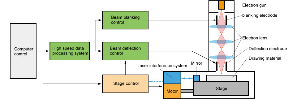


Components of Electron Beam Lithography [EBL] System
There are five central parts of the Electron beam lithography system. They are-
- An electron gun or a source that supplies electrons
- An electron column that focuses and shapes the electron beam
- A wafer handling system for automated feeding wafers to the system and uploading them after processing
- A mechanical stage that's utilized for placing the wafer under an electron beam
- A computer system controlling other components
Electron lithography and optical lithography employ negative and positive electron resists.
Electron Beam Lithography [EBL] has gradually become a highly suitable modern alternative type of lithography. One of the most favourable factors of EBL is that its cost-efficient and its applications have been very beneficial in the industry.

Benefits of using the E-beam lithography
- It allows the printing of difficult and complex patterns directly on different surfaces.
- This is quite useful technology with the elimination of diffraction problems
- The machine has a high resolution of about 20nm.
- Ensures a flexible technique to get different patterns done without any problems.
Advantages of Electron Beam Lithography
- EBL is used to manufacture tiny nanostructures with high accuracy and reliability at a resolution that's less than 10 nanometers.
- There's no requirement for a photomask to do the same.
- It is a suitable patterning method for the production of stamps utilized for nano-imprint lithography and a patterning method for product development.
- The electron systems are a lot slower than the Photolithography
- This machine and technology are expensive
- This method is associated with backscattering
Applications of Electron Beam Lithography
- The fabrication of integrated circuits (ICs).
- The manufacturing of microelectromechanical systems (MEMS).
- The production of photomasks.
- The creation of prototypes and models.
- The repair of damaged devices.
- The study of materials at the nanoscale.
Questions about Electron Beam Lithography (EBL)Q1 How does electron beam lithography work?
Ans: The EBL working principle is relatively simple and very similar to photolithography: A focused beam of electrons is scanned across a substrate covered by an electron-sensitive material (resist) that changes its solubility properties according to the energy deposited by the electron beam.
Q2. Why should one choose Electron Beam Lithography [EBL] over photolithography?
Ans. Like any other process, Electron Beam Lithography [EBL] has its own set of disadvantages too.
They are-
- Blanking or deflection error
- Shaping error
- Contamination
- Outgassing
- Backscattering calculation error
- Slower than Photolithography
Ans. There are three factors that affect the resolution of Electron Beam Lithography [EBL] are-
- Spot size
- Electrostatic repulsion happens due to the interaction of two electrons
- Scattering of electrons off the resistor substrate
Ans. Electron Beam Lithography [EBL] is a versatile technique that has a wide range of industrial applications.
Examples are:
- Optometrist-electronic devices.
- Microsystem techniques.
- Cyro-electric devices.


Comments
Post a Comment