MOS, SOI and FinFET Technology
The invention of vacuum tubes is what launched the electronics industry. These devices would control the flow of electrons in vacuum. But, after the second world war, it was observed that due to a huge number of discrete components, the complexity and power consumption of these devices were increasing significantly. As a result, the performance of the devices would keep going down. One of the examples is of a Boeing B-29 which during the war, would consist of 300-1000 vacuum tubes. Each additional component would reduce the reliability and increase troubleshooting time.
A major breakthrough came in 1947, when John Baden, William Shockley and Watter Brattain of Bell labs unveiled the first functioning point contact Germanium transistor. In 1950, Shockley developed the first Bipolar Junction Transistor (BJT). In comparison to a vacuum tube, transistors are more reliable, power efficient and of lesser size. The transistor is a 3-terminal device which can be viewed as an electrically controlled switch. One of the terminals acts as a control terminal. Ideally, if current is applied to the control terminal, the device will act as a close switch between the two terminals which otherwise behave as an open switch. In 1958, Jack Kilby of Texas Instruments built the first Integrated Circuit consisting of two bipolar transistors connected on a single piece of silicon, thereby initiating the “Silicon Age”. Early ICs used bipolar junction transistors. One of the drawbacks of BJT is a problem due to more static power dissipation. It means that power is drawn even when the circuit is not switching. This limits the maximum numbers of transistors that can be integrated into a single silicon chip.
In 1963, Frank Wanlass and C.T.Sah of Fairchild unveiled the first logic gate in which n-channel and p-channel transistors were used in a complementary symmetric circuit configuration. This is what is known as CMOS today. It draws almost zero static power dissipation.
Early ICs used NMOS technology, because the NMOS process was fairly simple, less expensive and more devices could be packed into a single chip compared to CMOS technology. The first microprocessor was announced by Intel in 1971.
As static power dissipation of NMOS transistor is more compared to CMOS, the power consumption of ICs became a serious issue in the 1980s as thousands of transistors were integrated into a single chip. Due to features like low power, reliable performance and high speed, CMOS technology would adopt and replace NMOS and bipolar technology for nearly all digital applications.
Throughout the next few years, CMOS scaling and improvement in processing technologies have led to continuous enhancement in circuit speeds, along with further improvement in packaging densities of chips and performance-to-cost ratios of microelectronics-based products.
Here, we discuss Bulk-Si CMOS technology, the need and importance of scaling, their various effects and associated solutions. We also address the physical scaling limits of transistor materials and any new materials used in advanced technology node. Nowadays, the industry is moving from the usage of planner transistor technology due to various limitations encountered below 32nm technology node. We discuss new device structures: SOI and FinFET which replaced planner bulk transistor.
II. MOSFET DEVICE OVERVIEW:
Here, we first discuss the basic structure, operation and important terms related to the core unit of CMOS i.e. MOSFET or simply MOS. The first successful MOS transistor would use metals for the gate material, SiO2 (oxide) for insulator and semiconductor for substrate. For that reason, this device was named MOS transistor. The name Field Effect Transistor (FET) refers to the fact that the gate is turned on and off by the transistor with an electric field passing through the gate oxide.
A. Structure of MOS:
Based on the type of conducting channel, two kinds of MOS structures are evident: n-channel and p-channel MOS. Here, we will only overview the NMOS transistor because both transistors are complementary in nature.
MOS transistor is a 4-terminal device having terminal drains, source, gate and body (substrate). Figure 1 shows the 3-dimentional structure of NMOS. The NMOS transistor is formed on a p-type silicon substrate (also called body). On the top center part of the device, a low resistivity electrode is formed which is separated from the body by an insulator. Generally, poly-silicons with heavy doping of either n-type or p-type is used as gate material. Here, silicon dioxide (SiO2 or simply oxide) is used as an insulator. By implanting donor impurities in two sides of the substrate, the source and the drain are formed. In Figure 1, these regions are denoted by n+ which indicate heavy doping of donor impurities. This heavy doping results in low resistivity for these regions.
If two n+ regions are biased at different potentials, the n+ region which is at lower potential will act as source while the other will act as drain. So, the drain and source terminals can be interchanged as per the potential applied to them. The region between source and drain is called the channel having width-W and length-L, which plays an important role in deciding the characteristics of an MOS transistor.
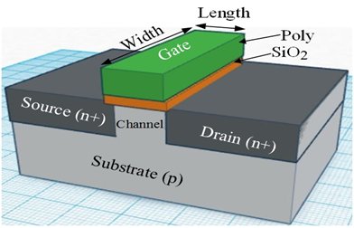
Figure 1. Structure of NMOS transistor
B. Why Polysilicon as Gate Material ?:
In the early days of semiconductor industry, the metal, Aluminum, was generally used as the preferred gate material of MOS. But later on, polysilicon has been preferred as gate material. Two main reasons were behind this transition to polysilicon as discussed below here.
The early MOS fabrication process started with the definition and doping of source and drain regions. Then, the gate mask was used which defines the gate oxide region which would later form the aluminum metal gate.
One of the major drawbacks of such a fabrication process is that if the gate mask is misaligned, it creates a parasitic overlap input capacitance Cgd and Cgs, as shown in figure-2(a). The capacitance Cgd is more harmful because it is a feedback capacitance. As a result of miller capacitance, there is a reduction in the transistor’s switching speed.
One of the solutions to the misalignment of the gate mask is what is known as a “Self-aligned Gate Process”. This process starts with the creation of the gate region followed by the creation of the drain and source regions using ion-implantation. The thin gate oxide under the gate acts as a mask for doping process preventing further doping under gate region (channel). So, this process makes the gate self-aligned with respect to the source and drain. As a result of all this, the source and drain do not extend under the gate. Thereby reducing Cgd and Cgs as shown in figure 2(b).
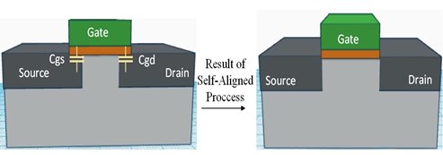
The doping process of the drain and source require very high temperature annealing methods (>8000*C). If aluminum is used as a gate material, it would melt under such high temperature. This is because the melting point of Al is approximately 660 degree C. But, if polysilicon is used as a gate material, it would not melt. Thus, the self-alignment process is possible with polysilicon gate. While in the case of Al-gate, it is not possible, which results in high Cgd and Cgs. Undoped polysilicon has very high resistivity, approximately 108 ohm/Cm. So, polysilicon is doped in such a way that its resistance is reduced.
The other reason for selecting poly is that the threshold voltage of MOS transistor is correlated with the work function difference between the gate and the channel. Earlier, metal gates were used when operating voltages were in the range of 3-5 volts. But, as the transistors were scaled down, which ensured that the operating voltages of the device were also brought down. A transistor with such high threshold voltage becomes non-operational under such conditions. Using metal as gate material resulted in high threshold voltage compared to polysilicon, since polysilicon would be of the same or similar composition as the bulk-Si channel. Also, as polysilicon is a semiconductor, its work function can be modulated by adjusting the level of doping.
C. Working Principle of MOS:
For MOS transistor, the gate voltage determines whether a current flow between the drain and source will happen or not. Let’s see further. When a sufficiently positive Vgs voltage is applied to the gates of NMOS, the positive charges are placed over the gate as shown in figure-3. These positive charges will repel the minority carriers of p-type substrate i.e. holes from the substrate, leaving behind negative charge acceptor ions which create depletion region. If we increase Vgs further, at some potential level it will even make the surface attractive to electrons. So, plenty of electrons are attracted to the surface. This situation is called inversion because the surface of p-type body normally has a large number of holes but the newer surfaces have a large numbers of electrons.
Drain-to-body and source-to-body are kept in reverse bias. Here in figure-3, source-to-body is kept at zero bias. As drain-to-body potential is more positive than source-to-body potential, the reverse bias across drain-to-body is larger resulting in deeper depletion under drain region compared to source side.
When positive potential across drain-to-source is applied, electrons flow from the source through the conducting channel and are drained by the drain. So, a positive current Id flows from drain-to-source.
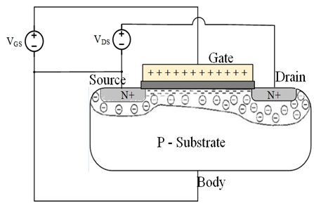
Figure 3. NMOS Transistor in inversion region
III. TECHNOLOGY SCALING MOTIVATION:
The demand for battery-operated portable gadgets have increased day by day with tons of applications including hearing aids, cellular phone, laptops etc. The “basic requirements” of such an application are less area, lower power consumption and cheaper development. For such portable devices, power dissipation is important because the power provided by the battery is rather limited. Unfortunately, battery technologies cannot be expected to improve the battery storage capacity by more than 30% every five years. This is not sufficient to handle the increasing power needed in portable devices.
In 1965, Gordon E. Moore predicted that the number of transistors in an Integrated Circuit will double every two years (widely known as Moore’s law). By making transistors smaller, more circuits can be fabricated on the silicon wafer and therefore, the circuit becomes cheaper. The reduction in channel length enables faster switching operations since less time is needed for the current to flow from drain to source. In other words, a smaller transistor leads to smaller capacitance. This causes a reduction in transistor delay. As dynamic power is proportional to capacitance, the power consumption also reduces. This reduction of transistor size is called scaling. Each time a transistor is scaled, we say a new technology node has been introduced. The minimum channel length of transistor is called the technology node. For example, 0.18 micrometer, 0.13 micrometer, 90 nanometer etc. The scaling improves cost, performance and power consumption with every new generation of technology.
IV. SMALL DIMENSIONS EFFECTS:
For long channel devices, “edge effects” along the four sides of the channel are really negligible. For long channel devices, the electric field lines are everywhere perpendicular to the surface of the channel. These electric fields are controlled by gate voltage and back gate voltage. But, for short channel devices, the drain and source structure are closer to the channel, especially when the longitudinal electric field in the channel comes into picture. The longitudinal electric field is controlled by drain-source voltage. The longitudinal electric field is parallel to the current flow direction. The device is called short channel device if channel length is not much larger than the sum of source and drain depletion widths.
In this section, we will discuss various undesirable effects arising as a result of two-dimensional potential distribution and high electric fields in the short channel.
A. Carrier Velocity Saturation & Mobility Degradation:
The electron drift velocity in the channel is proportional to the electric field for lower electric field values. These drift velocities tend to saturate at high electric fields. This is called velocity saturation. For short channel devices, the longitudinal electric field typically also increases. At such high electric fields, a velocity saturation occurs which affects I-V characteristics of the MOSFET. It has been observed that, for the same gate voltage, the saturation mode of MOSFET is achieved at smaller values of drain-source voltage and saturation current reductions.
Due to higher vertical electric fields, the carriers of the channel scatter off of the oxide interface. This results in the degradation of carrier mobility and the reduction in drain current.
B. Drain Induced Barrier Lowering:
Another short channel effect is called DIBL which refers to the reduction of threshold voltage at higher drain voltage. If the gate voltage is not sufficient to invert the surface (i.e. gate voltage < threshold voltage), the carriers in the channel will face a potential barrier that could block the flow. By increasing gate potential, we eliminate this potential barrier. But, for short channel devices, such a potential barrier is controlled by both Vgs and Vds. If this drain voltage is increased, the depletion region of the drain-body increases in size and extends under the gate. So, the potential barrier in the channel decreases leading to carriers (electrons) flowing between source and drain, even at Vgs lower than Vt. The concept of drain lowering the channel barrier and reducing the threshold voltage is called DIBL. This reduction in threshold voltage with channel length is called Vt roll-off. The current that flows under such conditions is called sub-threshold current (off-state current). DIBL causes drain current to increase with a rise in drain bias even in saturation mode.
C. Punch-through:
Punch-through is a severe case of barrier lowering. When the drain bias is increased, the depletion region surrounding the drain can extend further towards the source with two depletion regions merging. This condition is called punch-through. Under such conditions, the gate voltage loses its control over the drain current with rising drain current sharply. The punch-through effect increases with decreasing channel length. Due to punch-through, we cannot turn off the device, so the device becomes useless as shown in the figure 4.
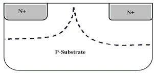
Figure 4. Punch through – merging of two depletion region
D. Hot Carrier Effects:
For smaller geometric devices, the electric field increases especially near the drain. As a result, the electrons (carriers) get a significant amount of energy which are called hot carriers.
Some of them get nearly enough energy which lead to impact ionization near drain, whereby new electron-hole pairs are generated. As an effect, it gives rise to drain-to-body current (Idb). A small numbers of hot electrons may tunnel through oxide and collect themselves by gate. While some hot carriers can even damage the oxide resulting in device degradation.
V. CONTROLLING SHORT CHANNEL EFFECTS:
We observed in the previous section that if channel length is small compared to the depletion regions, short channel effects become intolerable. This limits the further reduction achievable in gate length. To limit these effects, the depletion region width should be reduced with corresponding reduction in channel length. This can be achieved by either increasing channel doping concentration or increasing gate capacitance, or both. Gate capacitance determines the gate’s control over the channel. Equation 1 indicates that gate capacitance can be increased by scaling (reducing) gate oxide thickness. It has been observed that a device with thinner gate oxide has reduced depletion width, and hence, improved SCE characteristics.
COX = EOX / TOX (Equation - 1)
Where,
- COX : Gate Oxide Capacitance,
- EOX : Electric Field of oxide,
- TOX : Oxide Thickness
For Intel’s process nodes in the last 25 years, it has been observed that the oxide has been scaled roughly in proportion to the channel length in order to limit SCE. The relationship between channel length and oxide thickness for Intel’s technology nodes is given in Equation-2.
L = 45 X TOX (Equation - 2)
Where,
- L: Channel Length,
- TOX : Oxide Thickness
VI. POST TRADITIONAL SCALING INNOVAIONS:
A. Mobility Booster: Strained Silicon Technology
One of the key scaling problems in nano scale transistors is the mobility degradation caused by the larger vertical electric field. There are many ways to enhance transistor performance and mobility. One way is to use thin germanium film in the channel because germanium has higher carrier mobility. Another way is to use strained silicon by introducing mechanical strain in the channel.
The strained silicon technology involves physically stretching or compressing the silicon crystal using various means, which in turn, increases carrier (electrons/holes) mobility and enhances the performance of the transistor. For example, the hole mobility of PMOS can be increased when the channel is compressively stressed.
For making compressive strain in the silicon channel, the source and drain regions are filled with Si-Ge film by an epitaxial growth. Si-Ge typically comprises of 20% germanium and 80% silicon mixture. The number of Si and Ge atoms are equal to original Si atoms. Germanium atoms are larger than silicon atoms. So when a force is created, it pushes the channel and raises the hole mobility. Increasing the mobility of the semiconductor improves drive current and transistor speed.
The strained silicon techniques for MOS transistor were first used by Intel in their 90nm process technology in 2003. In this technology node, the Si-Ge source drain structure used for PMOS transistor induces compressive strain in the channel, improving current by 25%. While NMOS strain is introduced by adding high stress Si3N4 capping layer around transistor, improving current by 10%.
B. Gate Leakage Reduction: High-K Dielectric
The thickness of SiO2 (oxide) dielectric should be scaled in proportion to its channel length. The 65nm node, require Effective Oxide Thickness (EOT) of approximately 2.3nm (actual 1.6nm). But, if oxide thickness is reduced further below this point, the direct tunneling of carrier phenomena will be dominant. As a result of all this, the gate leakage increases to an unacceptable limit. So, the thickness limit for the oxide is approximately 1.6nm which is set by gate-to-channel tunneling leakage (also called quantum mechanical tunneling).
If we look at equation-1, the only option remaining is to select dielectric material having high dielectric constant (K) to increase the oxide capacitance. Since, thicker dielectric layers can be used, we get high gate-oxide capacitance. This thicker layer results in less carrier tunneling. SiO2 has dielectric constant of 3.9.
A breakthrough in gate oxide comes in 2007, the hafnium (HfO2) based High-K dielectric material was first introduced by Intel in its 45nm high volume manufacturing process. Hafnium material has dielectric constant of approximately 25 which is 6 times higher than SiO2.
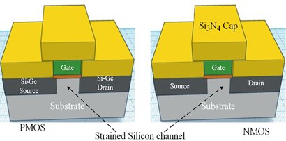
Figure 5. a) PMOS: Uniaxial Compressive Strain b) NMOS: Uniaxial Tensile Strain
EOT is given by equation 3. The equation 3 implies that 6nm thick HfO2 provides EOT of approximately 1nm.
EOT = ( 3.9 X TOX ) / K (Equation - 3)
Where,
- EOT: Effective Oxide Thickness,
- Tox: Oxide Thickness,
- K: Dielectric Constant of Material
C. Poly Depletion Elimination: Metal Gate
A depletion region forms at the interface of poly-silicon and gate oxide. As the device continues to scale down, this poly-silicon depletion becomes larger and a larger fraction of the equivalent oxide thickness will limit gate oxide capacitance. The negative effects of poly-depletion is due to reduction in inversion layer charge density and a degradation of device performance. So, apart from gate oxide thickness, poly depletion layer thickness also needs to be minimized.
Moreover, poly gates can also be incompatible with high-K dielectric because of effects such as threshold voltage pinning and photon scattering which make it difficult to obtain low threshold voltage and reduce the channel’s mobility.
One solution to eliminate poly-depletion effect is the use of metal gate instead of poly gate. A metal gate not only eliminates poly-depletion effect, but also enables the use of high-K dielectric.
Intel had first introduced 45nm node using high-K dielectric and metal gate technology. Different metals are used for NMOS and PMOS as different work-functions are required for NMOS and PMOS.
A transistor process flow starts with the deposition of high-K dielectric and dummy poly-silicon. After the high temperature annealing process, the inter layer dielectric is deposited and polished to expose poly-silicon. Then, a dummy poly-silicon is removed. At last, PMOS and then NMOS work function metals are deposited in the gate trenches.
VII. NEW INNOVATIVE DEVICE STRUCTURES:
For conventional MOS structure, as the channel length shrinks, the gate does not have full control over the channel which is not desirable. One of its effects is to cause more sub-threshold leakage from drain to source, which is not good from power consumption point of view. In conventional MOS, the gate cannot control leakage path which is far removed from the it. This can be improved using various MOS structures which allow the scaling of a transistor beyond conventional MOS scaling limit. In this section, we will discuss two new MOS structures, SOI and FinFET. The main objective of both the structures is to maximize gate-to-channel capacitance and minimize drain-to-channel capacitance.
A. Silicon-On-Insulator (SOI):
The main difference between conventional MOS structure and SOI MOS structure is that SOI device has a buried oxide layer, which isolates the body from the substrate. As shown in the Figure 7, SOI transistor is a planner device.
The fabrication process of SOI MOS is similar to bulk MOS (conventional MOS) process except for the starting silicon wafer. SOI wafers have three layers; 1. Thin surface layer of silicon (where the transistors are formed). 2. An underlying layer of insulating material. 3. A support or "handle" silicon wafer.
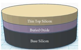
Figure 6. SOI Wafer
The basic idea behind buried oxide layer is, that it will reduce the parasitic junction capacitance. And the smaller the parasitic capacitance, the faster will the transistor work. Giving higher performance. Due to BOX layer, there is no unwanted leakage paths which are far from the gate. This leads to lower power consumption.
Depending on the condition of the thin body during operation, SOI devices are categorized as Partially Depleted (PD) SOI and Fully Depleted (FD) SOI. Compared to PD SOI, FD SOI have very thin body structures, hence the body is fully depleted during operation. This FD SOI also called Ultra-Thin-Body SOI. For PD SOI, body is 50 nm to 90 nm thick. While for FD SOI, the body is about 5 nm to 20 nm thick.
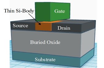
Figure 7. Structure of SOI FET
Advantages of SOI Devices:
- Owing to oxide layer isolation, the drain/source parasitic capacitances are reduced. So, the delay and dynamic power consumption of the device is lower compared to bulk CMOS.
- Due to an oxide layer, the threshold voltage is less dependent on back gate bias compared to bulk CMOS. This makes the SOI device more suitable for low power applications.
- Sub-threshold characteristics of SOI devices are better, so leakage currents are smaller.
- SOI devices have no latch-up problems.
Drawbacks of SOI Devices:
- One of the drawbacks of PD SOI device is that they suffer from history effect. In PD SOI, as the body becomes thicker, a floating body is evident. So, the body voltage is dependent on the previous state of the device. This floating body voltage can change the threshold voltage of the device. It could cause significant mismatch between two identical transistors.
- The other problem with an SOI device is self-heating. In SOI device, the active thin body is on silicon oxide which is good thermal insulator. During an operation, the power consumed by the active region cannot be dissipated easily. As a result, the temperature of the thin body rises which decreases the mobility and current of the device.
- One of the challenges with FD SOI is the difficulty in manufacturing thin body SOI wafers.
B. FinFET:
Former TSMC CTO and Berkeley professor Chenming Hu and his team presented the concept of FinFET in 1999 and UTB-SOI (FD SOI) in 2000. The main principle behind both the structures is a thin body, so the gate capacitance is closer to whole channel. The body is very thin, around 10nm or less. So, there is no leakage path which is far from the gate. The gate can effectively control the leakage.
The basic structure of FinFET which they proposed would be a channel controlled by more than one side of channel. One of the Double-Gate Structures is shown in Figure 8.
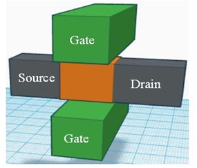
Figure 8. Double Gate Structure
Modern FinFETs are 3D structures as shown in the Figure 9 also called tri-gate transistor. FinFETs can be implemented either on bulk silicon or SOI wafer. This FinFET structure consists of thin (vertical) fin of silicon body on a substrate. The gate is wrapped around the channel providing excellent control from three sides of the channel. This structure is called the FinFET because its Si body resembles the back fin of a fish.
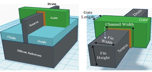
Figure 9. Fin-FET Structure
In bulk-MOS (planner MOS), the channel is horizontal. While in FinFET channel, it is vertical. So for FinFET, the height of the channel (Fin) determines the width of the device. The perfect width of the channel is given by Equation 4.
Width of Channel = 2 X Fin Height + Fin Width (Equation-4)
(Source: Synopsys)
The drive current of the FinFET can be increased by increasing the width of the channel i.e. by increasing the height of the Fin. We can also increase the device drive current by constructing parallel multiple fins connected together as shown in the Figure 10. It implies that for a FinFET, the arbitrary channel width is not possible, since it is always a multiple of fin height. So, effective width of the device becomes quantized. While in planner devices, there is the freedom to choose the device’s drive strength by varying channel width.
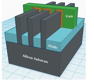
Figure 10. Multi-Fin FinFET Structure
In conventional MOS, a doping is inserted into the channel, reducing the various SCEs and ensuring high Vth. While in FinFET, the gate structure is wrapped around the channel and the body is thin, providing better SCEs, so channel doping becomes optional. It implies that FinFET suffers less from dopant-induced variations. Low channel doping also ensures better mobility of the carriers inside the channel. Hence, higher performance. One thing noticed over here is that both FinFET and SOI technologies have introduced Body Thickness as a new scaling parameter.
FinFET technology provides numerous advantages over bulk CMOS, such as higher drive current for a given transistor footprint, hence higher speed, lower leakage, hence lower power consumption, no random dopant fluctuation, hence better mobility and scaling of the transistor beyond 28nm.
VIII. SOI VS FINFET:
As SOI technology is very close to planner bulk technology, it does not require much investment in Fab. So, existing bulk technology libraries can easily be converted to SOI libraries. Another advantage of SOI over FinFET is, that it has good back gate bias option. By creating back gate region below BOX, we can also control Vt. This make it suitable for low power applications.
The primary limitation of SOI technology is the cost of an SOI wafer which is higher than a bulk Silicon wafer because it is very difficult to control the tin silicon film throughout the wafers. Another stumbling block for SOI adoption is a limited number of SOI wafer suppliers. According to Intel, SOI wafer adds approximately 10% to the total process cost.
In comparison to SOI, FinFET has higher drive current. Moreover in FinFET, the strain technology can be used to increase carrier mobility.
One of the downsides of FinFET is its complex manufacturing process. According to Intel, the cost of FinFET manufacturing can increase by 2-3% over bulk.
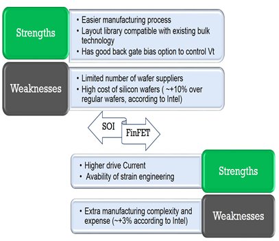
Figure 11. Strengths-Weaknesses of SOI and FinFET
IX. SOI-FINFET IN MICROELECTRONICS INDUSTRY:
Intel introduced Trigate FETs at the 22 nm node in the Ivy-Bridge processor in 2012. Other foundries that are offering FinFET technology are TSMC, Global Foundry, and Samsung. In 2014, TSMC announced that it has produced its first fully functional ARM-based networking processor with 16nm FinFET technology.
STMicroelectronics released its first FD-SOI chips for mobile processor at 28nm in 2012. Foundries that are offering FD-SOI technology are IBM, Global Foundry, and Samsung. Some of the products using SOI technology are AMD's processor, PowerPC microprocessor and Sony's PlayStation.


Comments
Post a Comment