Molecular-Beam Epitaxy
Molecular-Beam Epitaxy
Molecular-beam epitaxy (MBE) is an epitaxy method for thin-film deposition of single crystals. MBE is widely used in the manufacture of semiconductor devices, including transistors, and it is considered one of the fundamental tools for developing nanotechnologies. MBE is used to fabricate diodes and MOSFETs (MOS field-effect transistors) at microwave frequencies and to manufacture the lasers used to read optical discs (such as CDs and DVDs).
History
Original ideas of the MBE process were first established by K. G. Günther. Films he deposited were not epitaxial, but were deposited on glass substrates. With the development of vacuum technology, the MBE process was demonstrated by John Davey and Titus Pankey who succeeded in growing GaAs epitaxial films on single crystal GaAs substrates using Günther's method. Major subsequent development of MBE films was enabled by J.R. Arthur's investigations of the kinetic behavior of growth mechanisms and Alfred Y. Cho's in situ observation of the MBE process using reflection high-energy electron diffraction (RHEED) in the late 1960s.


Figure:- A simple sketch showing the main components and rough layout and concept of the main chamber in a molecular-beam epitaxy system
Molecular beam epitaxy (MBE) is an experimental technique utilized for layer-by-layer growth of thin films of various quantum materials. Out of the variety of thin film growth techniques available, MBE is considered to be one of the cleanest, but also one of the most technically challenging and demanding, as MBE growth takes place in an ultra-high vacuum (UHV) environment.
A typical MBE experimental setup consists of two or more Knudsen effusion cells (K-cells), located at the bottom of a UHV chamber and aligned towards the center of the chamber where a sample holder with a substrate is located (Figure 1). Each individual K-cell contains a different element in ultra-pure solid form (i.e. elemental 99.999% Selinum, Bismuth, etc.) which can be used in the thin film synthesis. The process of MBE growth starts by heating the K-cells to appropriate temperatures until the elements in each cell reach a sublimation point. Then, the shutters are opened and physical vapor from each K-cell diffuses though the chamber until it reaches the substrate where it gets deposited, and the thin film gets formed. The final composition and stoichiometry of the film will depend on the temperature and surface atomic structure of the substrate, as well as the flux ratios of individual components reaching the substrate. For more uniform growth, the substrate can be continuously rotated at low rotation speeds (~1-2 rotations per minute) by utilizing a stepper motor attached to the magnetic manipulator.
To characterize the samples in-situ during growth, we use reflection high-energy electron diffraction (RHEED). Electrons emitted from the RHEED gun (Figure 1) incident at a very low angle with respect to the sample surface are diffracted, and the resulting diffraction pattern is observed on the screen. This pattern can reveal: (1) quality of the film surface, and (2) film thickness down to a single monolayer.
What is molecular beam epitaxy?
To make an interesting new crystal using MBE, you start off with a base material called a substrate, which could be a familiar semiconductor material such as silicon, germanium, or gallium arsenide. First, you heat the substrate, typically to some hundreds of degrees (for example, 500–850°C or about 930–1560°F in the case of gallium arsenide).
Then you fire relatively precise beams of atoms or molecules (heated up so they're in gas form) at the substrate from "guns" called effusion cells. Each effusion cell is open at one end and consists of a tapering crucible (a kind of heat-resistant cup) filled with the material it's going to "fire," an electrically controlled heater, and a thermocouple for measuring and regulating its temperature. The number of cells depends on the complexity of the crystal being produced; there can be as many as 8–14 of them. Like the substrate, the cells are heated to high temperatures—a maximum of about 1500–1600°C or so (2700–2900°F).

Artwork: A typical effusion cell is a cone-shaped, electrically heated crucible, usually made from pyrolitic boron nitride (PBN), which can withstand high temperatures and low pressures. Its temperature is measured and controlled using a thermocouple, mounted at its base. The evaporant (the substance being fired out as a molecular beam) sits at the bottom of the crucible. A heat sink (blue) and radiative insulation (yellow) help to stop nearby effusion cells from affecting one another.
You need one cell for each different beam, shooting a different kind of molecule at the substrate, depending on the nature of the crystal you're trying to create. The molecules land on the surface of the substrate, condense, and build up very slowly and systematically in ultra-thin layers, so the complex, single crystal you're after grows one atomic layer at a time. (Very slowly means very slowly, typically at a rate of a few microns, or fractions of microns, per hour.) [5] That's why MBE is an example of what's called thin-film deposition. Since it involves building up materials by manipulating atoms and molecules, it's also a perfect example of what we mean by nanotechnology.
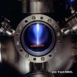
Photo: Molecular beam epitaxy (MBE) in action. MBE takes place in ultra-high vacuum (UHV) chambers like this, at temperatures of around 500°C (932°F), to ensure a totally clean, dust-free environment; the slightest contamination could ruin the crystal. Photo by Jim Yost courtesy of US DOE/NREL (U.S. Department of Energy/National Renewable Energy Laboratory).
One reason that MBE is such a precise way of making a crystal is that it happens in highly controlled conditions: extreme cleanliness and what's called an ultra-high vacuum (UHV), so no dirt particles or unwanted gas molecules can interfere with or contaminate the crystal growth. "Extreme cleanliness" means even cleaner than the conditions used in normal semiconductor manufacture; an "ultra-high vacuum" means the pressure is so low that it's at the limit of what's easily measurable—as little as one hundred trillionth of atmospheric pressure.
That's pretty much MBE in a nutshell. If you want a really simply analogy, it's a little bit like the way an inkjet printer makes layers of colored print on a page by firing jets of ink from hot guns. In an inkjet printer, you have four separate guns firing different colored inks (one for cyan ink, one for magenta, one for yellow, and one for black), which slowly build up a complex colored image on the paper. In MBE, separate beams fire different molecules and they build up on the surface of the substrate, albeit more slowly than in inkjet printing—MBE can take hours! Epitaxially simply means "arranged on top of," so all molecular beam epitaxy really means is using beams of molecules to build up layers on top of a substrate.
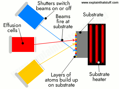
A simple diagram showing how molecular beam epitaxy works
Photo: Molecular beam epitaxy (MBE) means creating a single crystal by building up orderly layers of molecules on top of a substrate (base layer). This bit of apparatus is called a growth chamber. It's only one part of an MBE machine, which typically includes multi chambers (introduction and extraction chambers, two or more growth chambers, an analysis chamber, and a preparation chamber), all kept at ultra-high vacuum (UHV).
Typical uses
You might want to create a semiconductor laser for a CD player, or an advanced computer chip, or a low-temperature superconductor. Or maybe you want to build a solar-cell by depositing a thin film of a photovoltaic material (something that creates electricity when light falls on it) onto a substrate. In short, if you're designing a really precise thin-film device for computing, optics, or photonics (using light beams to carry and process signals in a similar way to electronics), MBE is one of the techniques you'll probably consider using. Apart from industrial processes, it's also used in all kinds of advanced nanotechnology research.
Advantages and Disadvantages
Why use MBE rather than some other method making a crystal? It's particularly good for making high-quality (low-defect, highly uniform) semiconductor crystals from compounds (based on elements in groups III(a)–V(a) of the periodic table), or from a number of different elements, instead of from a single element. It also allows extremely thin films to be fabricated in a very precise, carefully controlled way. Unfortunately, it does have some drawbacks too. It's a slow and laborious method (crystal growth rate is typically a few microns per hour), which means it's more suited for scientific research laboratories than high-volume production, and the equipment involved is complex and very expensive (partly because of the difficulty of achieving such clean, high-vacuum conditions).
Who invented molecular beam epitaxy?
The basic MBE technique was developed around 1968 at Bell Laboratories by two American physicists, Chinese-born Alfred Y. Cho and John R. Arthur, Jr. Important contributions were also made by other scientists, such as Japanese-born physicist Leo Esaki (who won the 1973 Nobel Prize in Physics for his work on semiconductor electronics) and Ray Tsu, working at IBM. Since then, many other researchers have developed and refined the process. Alfred Cho was awarded the inaugural Nanotechnology International Prize, RUSNANOPRIZE-2009, for his work in developing MBE.
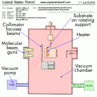
Artwork (below): A drawing taken from John R. Arthur, Jr.'s original molecular beam epitaxy patent, filed in 1968 and granted in 1971. Artwork courtesy of US Patent and Trademark office. You can find more details in US Patent #3,615,931: Technique for Growth of Epitaxial Compound Semiconductor Films (via Google Patents).


Comments
Post a Comment